El Transistor NPN estructura y aplicaciones HETPRO/TUTORIALES
Simbol: Nama: Deskripsi: Transistor Bipolar NPN: Memungkinkan aliran arus ketika potensi tinggi di basis (tengah) Transistor Bipolar PNP: Memungkinkan aliran arus ketika potensi rendah di basis (tengah) Transistor Darlington: Terbuat dari 2 transistor bipolar. Memiliki keuntungan total dari produk dari setiap keuntungan. Transistor JFET-N
Electronic Transistor and Transistor symbols « Electrical and Electronic Free Learning Tutorials
Transistor adalah?☑️ Berikut Ulasan Lengkap Mengenai pengertian dan fungsi transistor ☑️ Simbol Transistor, dan Cara kerja transistor berikut contohnya☑️ Hal yang menarik ketika Kita membahas tentang transistor, Ketika ditemukan pada tahun 1947, transistor tidak benar-benar melakukan apa pun yang belum pernah dilakukan sebelumnya.

Transistor Schematic Symbol ClipArt Best
What is a NPN Transistor. An NPN transistor is the most commonly used bipolar junction transistor, and is constructed by sandwiching a P-type semiconductor between two N-type semiconductors. An NPN transistor has three terminals- a collector, emitter and base. The NPN transistor behaves like two PN junctions diodes connected back to back.
Transistor Pengertian, Simbol, dan 4 Karaktertistiknya
Simbol Transistor JFET Kanal N. Termasuk kedalam transistor efek medan/ Field Effect Transistor (FET) jenis transistor Junction Field Effect Transistor terdiri dari kanal N dan kanal P. Karakteristik keluaran dari JFET adalah ketika gate diberikan voltase 0, maka arus pada pin drain dan source ( Ids ) akan mengalir, sedangkan jika diberi tegangan minus maka transistor akan menyumbat/ tidak.
Simbolos Transistores Images
Bipolar transistors are 3-terminal devices with the schematic symbol of a bipolar transistor marked with the letters of "C", "B" and "E" corresponding to the terminals of Collector, Base and Emitter respectively. Conventional current flows through a bipolar transistor from the Emitter terminal to the Collector terminal while the Base terminal controls the amount of current flow.
The Most Common Schematic Symbols Used in Electronics
Size comparison of bipolar junction transistor packages, including (from left to right): SOT-23, TO-92, TO-126, and TO-3 Metal-oxide-semiconductor field-effect transistor (MOSFET), showing gate (G), body (B), source (S) and drain (D) terminals. The gate is separated from the body by an insulating layer (white). A transistor is a semiconductor device used to amplify or switch electrical.
Transistors, Hybrid Circuit Schematic Symbols Electronics Textbook
Transistors, Bipolar. There are not too many circuit symbols for bipolar transistors. There are of course different circuit symbols to indicate NPN and PNP transistors. In addition to this, some transistor circuit symbols have the circle around them and others not. Those without are widely used in the circuits detailing the internal circuitry.

Simbol Transistor ClipArt Best
The pinout on the physical package does not always follow the electronic symbol. You therefore need the documentation of the transistor to figure out how the pins are organised. For example, the BC546, BC547, BC548, and BC549 transistors come in a TO-92 package. When the flat side is facing you, the pins are collector, base, and emitter.
Transistor Symbole · Images vectorielles gratuites sur Pixabay
Electronic symbol. An electronic symbol is a pictogram used to represent various electrical and electronic devices or functions, such as wires, batteries, resistors, and transistors, in a schematic diagram of an electrical or electronic circuit. These symbols are largely standardized internationally today, but may vary from country to country.

Simbol Transistor ClipArt Best
Bipolar junction transistor (BJT) symbol. The emitter, base, and collector pins of transition that are added in the symbol of BJT. The line having a direction to the emitter is used to show the collectors and the arrow in towards the outer direction is used to show the emitter. The connecting emitter and collector is the base.
Transistor Pengertian, Fungsi, Jenis, Simbol, Cara Kerja & Contoh Rangkaian ServiceSparePart
Video transcript. in this video let's look at the circuit symbol of a transistor we've already seen that there are two kinds of transistors one is the NPN where a p-type is sandwiched between two n types and we also have a PNP transistor where a P an n-type is sandwiched between two P types and in the previous video we even saw what their names.

ELECTRONIC TRANSISTOR SYMBOLS
JFET transistors stand for junction field effect transistors. JFETs are voltage-controlled transistors composed of 3 terminals: the gate, the drain, and the source. N-channel JFETS are composed of a majority of electrons, while P-channel JFETs are composed of a majority of holes. This internal composition difference differs their operation.
Simbolos Transistores Images
Transistor Adalah ? Pengertian dan Fungsi transistor beserta jenis dan gambar simbolnya☑️ Cara kerja transistor lengkap dengan contohnya☑️ Transistor merupakan komponen yang kerap ada pada berbagai rangkaian elektronik, baik yang sederhana ataupun yang kompleks. Bahan-bahan yang biasa digunakan untuk membuatnya yakni silicon, gallium, arsenide, dan germanium.
Transistor Symbols ClipArt Best
Transistor Symbols. The Transistor is a semiconductor device provided with three terminals called base, emitter and collector. It is used to work in electronic circuits as a rectifier, amplifier and switch. These symbols can be represented inside a circle. MOSFET Transistors Picture gallery Download symbols + Info Transistors.
Gambar Simbol Transistor cari
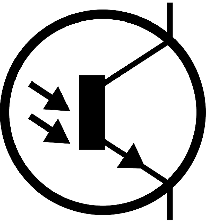
The phototransistor is a semiconductor light sensor formed from a basic transistor with a transparent cover that provides much better sensitivity than a photodiode. It is basically a 3-layer semiconductor device which has a light-sensitive base region. The base senses the light and converts it into the current which flows between the collector and the. A PNP transistor is a bipolar junction transistor constructed by sandwiching an N-type semiconductor between two P-type semiconductors. A PNP transistor has three terminals - a Collector (C), Emitter (E) and Base (B). The PNP transistor behaves like two PN junctions diodes connected back to back. These back to back PN junction diodes are.Simbol Transistor Gudang Ilmu